- 您现在的位置:买卖IC网 > Sheet目录3871 > PIC18F2221T-I/SS (Microchip Technology)IC PIC MCU FLASH 2KX16 28SSOP
2009 Microchip Technology Inc.
DS39689F-page 71
PIC18F2221/2321/4221/4321 FAMILY
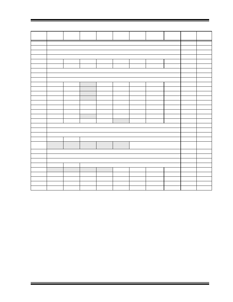
SPBRGH
EUSART Baud Rate Generator Register High Byte
0000 0000
SPBRG
EUSART Baud Rate Generator Register Low Byte
0000 0000
RCREG
EUSART Receive Register
0000 0000
TXREG
EUSART Transmit Register
0000 0000
TXSTA
CSRC
TX9
TXEN
SYNC
SENDB
BRGH
TRMT
TX9D
0000 0010
RCSTA
SPEN
RX9
SREN
CREN
ADDEN
FERR
OERR
RX9D
0000 000x
EEADR
EEPROM Address Register
EEDATA
EEPROM Data Register
EECON2
EEPROM Control Register 2 (not a physical register)
EECON1
EEPGD
CFGS
—
FREE
WRERR
WREN
WR
RD
IPR2
OSCFIP
CMIP
—
EEIP
BCLIP
HLVDIP
TMR3IP
CCP2IP
11-1 1111
PIR2
OSCFIF
CMIF
—
EEIF
BCLIF
HLVDIF
TMR3IF
CCP2IF
00-0 0000
PIE2
OSCFIE
CMIE
—
EEIE
BCLIE
HLVDIE
TMR3IE
CCP2IE
00-0 0000
IPR1
PSPIP(2)
ADIP
RCIP
TXIP
SSPIP
CCP1IP
TMR2IP
TMR1IP
1111 1111
PIR1
PSPIF(2)
ADIF
RCIF
TXIF
SSPIF
CCP1IF
TMR2IF
TMR1IF
0000 0000
PIE1
PSPIE(2)
ADIE
RCIE
TXIE
SSPIE
CCP1IE
TMR2IE
TMR1IE
0000 0000
OSCTUNE
INTSRC
PLLEN(3)
—
TUN4
TUN3
TUN2
TUN1
TUN0
00-0 0000
TRISE(2)
IBF
OBF
IBOV
PSPMODE
—
TRISE2
TRISE1
TRISE0
0000 -111
TRISD(2)
PORTD Data Direction Control Register
1111 1111
TRISC
PORTC Data Direction Control Register
1111 1111
TRISB
PORTB Data Direction Control Register
1111 1111
TRISA
TRISA7(5)
TRISA6(5)
PORTA Data Direction Control Register
1111 1111
LATE(2)
—
PORTE Data Latch Register
(Read and Write to Data Latch)
---- -xxx
LATD(2)
PORTD Data Latch Register (Read and Write to Data Latch)
xxxx xxxx
LATC
PORTC Data Latch Register (Read and Write to Data Latch)
xxxx xxxx
LATB
PORTB Data Latch Register (Read and Write to Data Latch)
xxxx xxxx
LATA
LATA7(5)
LATA6(5)
PORTA Data Latch Register (Read and Write to Data Latch)
xxxx xxxx
PORTE
—
—RE3(4)
RE2(2)
RE1(2)
RE0(2)
---- xxxx
PORTD(2)
RD7
RD6
RD5
RD4
RD3
RD2
RD1
RD0
xxxx xxxx
PORTC
RC7
RC6
RC5
RC4
RC3
RC2
RC1
RC0
xxxx xxxx
PORTB
RB7
RB6
RB5
RB4
RB3
RB2
RB1
RB0
xxxx xxxx
PORTA
RA7(5)
RA6(5)
RA5
RA4
RA3
RA2
RA1
RA0
xx0x 0000
TABLE 6-2:
REGISTER FILE SUMMARY (PIC18F2221/2321/4221/4321) (CONTINUED)
File Name
Bit 7
Bit 6
Bit 5
Bit 4
Bit 3
Bit 2
Bit 1
Bit 0
Value on
POR, BOR
Details on
page:
Legend:
x = unknown, u = unchanged, — = unimplemented, q = value depends on condition
Note
1:
The SBOREN bit is only available when the BOREN<1:0> Configuration bits = 01; otherwise, it is disabled and reads as ‘0’. See
Section 5.4 “Brown-out Reset (BOR)”.
2:
These registers and/or bits are not implemented on 28-pin devices and are read as ‘0’. Reset values are shown for 40/44-pin devices;
individual unimplemented bits should be interpreted as ‘-’.
3:
The PLLEN bit is only available in specific oscillator configurations; otherwise, it is disabled and reads as ‘0’. See Section 3.6.4 “PLL in
INTOSC Modes”.
4:
The RE3 bit is only available when Master Clear Reset is disabled (MCLRE Configuration bit = 0); otherwise, RE3 reads as ‘0’. This bit is
read-only.
5:
RA6/RA7 and their associated latch and direction bits are individually configured as port pins based on various primary oscillator modes.
When disabled, these bits read as ‘0’.
6:
Bit 7 and bit 6 are cleared by user software or by a POR.
发布紧急采购,3分钟左右您将得到回复。
相关PDF资料
PIC18F4682T-I/ML
IC PIC MCU FLASH 40KX16 44QFN
PIC24HJ128GP306T-I/PT
IC PIC MCU FLASH 128KB 64TQFP
PIC24FJ96GA008T-I/PT
IC PIC MCU FLASH 96KB 80TQFP
PIC24FJ64GA010T-I/PT
IC PIC MCU FLASH 64KB 100TQFP
PIC24FJ64GA008T-I/PT
IC PIC MCU FLASH 64KB 80TQFP
PIC18LF4450T-I/PT
IC PIC MCU FLASH 8KX16 44TQFP
PIC18LF2450T-I/ML
IC PIC MCU FLASH 8KX16 28QFN
PIC16F1937-I/ML
IC PIC MCU FLASH 512KX14 44-QFN
相关代理商/技术参数
PIC18F2320-E/SO
功能描述:8位微控制器 -MCU 8KB 512 RAM 25 I/O RoHS:否 制造商:Silicon Labs 核心:8051 处理器系列:C8051F39x 数据总线宽度:8 bit 最大时钟频率:50 MHz 程序存储器大小:16 KB 数据 RAM 大小:1 KB 片上 ADC:Yes 工作电源电压:1.8 V to 3.6 V 工作温度范围:- 40 C to + 105 C 封装 / 箱体:QFN-20 安装风格:SMD/SMT
PIC18F2320-E/SP
功能描述:8位微控制器 -MCU 8KB 512 RAM 25 I/O RoHS:否 制造商:Silicon Labs 核心:8051 处理器系列:C8051F39x 数据总线宽度:8 bit 最大时钟频率:50 MHz 程序存储器大小:16 KB 数据 RAM 大小:1 KB 片上 ADC:Yes 工作电源电压:1.8 V to 3.6 V 工作温度范围:- 40 C to + 105 C 封装 / 箱体:QFN-20 安装风格:SMD/SMT
PIC18F2320-I/SO
功能描述:8位微控制器 -MCU 8KB 512 RAM 25 I/O RoHS:否 制造商:Silicon Labs 核心:8051 处理器系列:C8051F39x 数据总线宽度:8 bit 最大时钟频率:50 MHz 程序存储器大小:16 KB 数据 RAM 大小:1 KB 片上 ADC:Yes 工作电源电压:1.8 V to 3.6 V 工作温度范围:- 40 C to + 105 C 封装 / 箱体:QFN-20 安装风格:SMD/SMT
PIC18F2320-I/SO
制造商:Microchip Technology Inc 功能描述:IC 8BIT FLASH MCU 18F2320 SOIC28
PIC18F2320-I/SP
功能描述:8位微控制器 -MCU 8KB 512 RAM 25 I/O RoHS:否 制造商:Silicon Labs 核心:8051 处理器系列:C8051F39x 数据总线宽度:8 bit 最大时钟频率:50 MHz 程序存储器大小:16 KB 数据 RAM 大小:1 KB 片上 ADC:Yes 工作电源电压:1.8 V to 3.6 V 工作温度范围:- 40 C to + 105 C 封装 / 箱体:QFN-20 安装风格:SMD/SMT
PIC18F2320-I/SP
制造商:Microchip Technology Inc 功能描述:IC 8BIT FLASH MCU 18F2320 SDIL28
PIC18F2320T-I/SO
功能描述:8位微控制器 -MCU 8KB 512 RAM 25 I/O RoHS:否 制造商:Silicon Labs 核心:8051 处理器系列:C8051F39x 数据总线宽度:8 bit 最大时钟频率:50 MHz 程序存储器大小:16 KB 数据 RAM 大小:1 KB 片上 ADC:Yes 工作电源电压:1.8 V to 3.6 V 工作温度范围:- 40 C to + 105 C 封装 / 箱体:QFN-20 安装风格:SMD/SMT
PIC18F2321-E/ML
功能描述:8位微控制器 -MCU 8KB FLSH 512BRAM 8B nanoWatt RoHS:否 制造商:Silicon Labs 核心:8051 处理器系列:C8051F39x 数据总线宽度:8 bit 最大时钟频率:50 MHz 程序存储器大小:16 KB 数据 RAM 大小:1 KB 片上 ADC:Yes 工作电源电压:1.8 V to 3.6 V 工作温度范围:- 40 C to + 105 C 封装 / 箱体:QFN-20 安装风格:SMD/SMT